Back to Faculty Directory
John Ekerdt
Professor Emeritus
Norbert Dittrich-Welch Chair Emeritus in Chemical Engineering
Department Research Areas
Advanced Materials, Polymers and Nanoengineering
Energy
Educational Qualifications
Ph.D., Chemical Engineering, University of California Berkeley (1979)
B.S., Chemical Engineering, University of Wisconsin (1974)
Focus
Surface and materials chemistry of metal and oxide thin films and hetero-structures – alone and integrated with semiconductors; film nucleation; film growth by atomic layer deposition and film removal by atomic layer etching; area-selective growth phenomena.
  |
  |
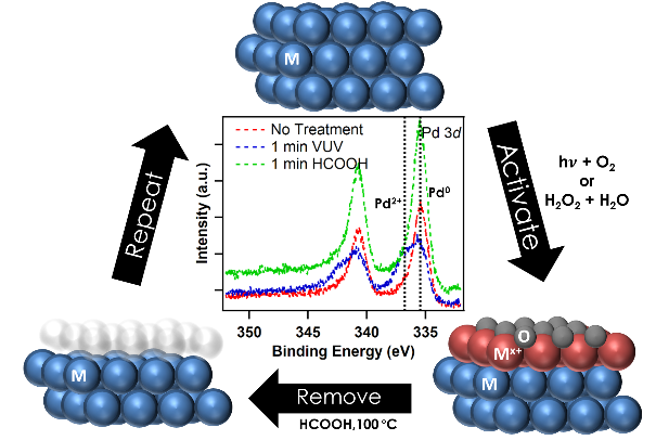
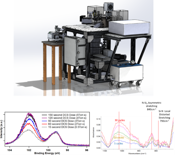
| Figure 1. We study anisotropic atomic layer etching of metals, such as Pd. Experiments seek conditions that limit the amount (depth) of oxide formed using vacuum ultraviolet light and various oxidants. The oxidized layers are removed thermally with formic acid. | Figure 2. The experimental facility is used to understand how plasma power, frequency, and gas affect reactive radical formation, and to follow the surface adsorbates in situ and how they change with plasma conditions. XPS shows ALD dose saturation and in situ FTIR shows increasing intensity of Si-N vibrational modes with cycles. |
Research
We study advanced materials to enable next generation technology. Projects explore the surface and materials chemistry of metal and oxide thin films and hetero-structures – alone and integrated with semiconductors. We seek to understand and describe film nucleation, film growth by atomic layer deposition and film removal by atomic layer etching, and area-selective growth phenomena. The programs are motivated by applications in electronic materials, energy and sensors. The research programs are highly interdisciplinary and involve collaborations with faculty in chemical engineering, physics and electrical engineering, and researchers in industry.
The research on area selective atomic layer deposition (AS-ALD) explores how to passivate the surfaces using organic blocking layers that either self-assemble or are lithographically patterned, the robustness of the blocking layer and how the blocking layer fails. In parallel we study the chemical nature of the active surface for ALD so thin and uniform films can be deposited in the active regions. AS-ALD projects are exploring metals, simple binary metal oxides, and ternary oxides, and the growth of amorphous and crystalline films. Inevitably a metal or metal oxide begins to nucleate and grow on the passivated regions and it becomes necessary to remove this unwanted material while minimizing removal from the intended growth regions. Atomic layer etching (ALE) is one way to remove one to several atomic layers of the deposited material. The image in Fig. 1 illustrates studies in our group into the chemistry that leads to anisotropic metal ALE.
The research on perovskite films seeks to understand the chemical reactions responsible for atomic layer deposition growth and the interfacial reactions responsible for forcing the films to grow in a crystalline form. Studies with perovskites explore homoepitaxy and heteroepitaxy using ALD and the role of the growth surface termination to realize two dimensional epitaxial growth and control the properties in the perovskite layer. These studies explore the monolithic integration of functional oxides with silicon to allow for silicon photonics and germanium to allow for integrated heterostructures on the same platform as the integrated circuits. We also study plasma-enhanced ALD of silicon nitrides and silicon carbonitrides (Fig. 2); this collaborative program is informed by first principles modeling studies in the G. S. Hwang group. Model predictions are used to guide the experimental studies, which in turn are used to validate and refine the models.
Awards & Honors
- Fellow of the American Association for the Advancement of Science, 2012
- American Society for Engineering Education Chemical Engineering Division Chemstations Award, 2012
- Fellow of the American Institute of Chemical Engineers (AIChE), 2006
- Joe J. King Professional Engineering Achievement Award, College of Engineering, University of Texas, 2005
- Hamilton Book Awards, for Chemical Reactor Analysis and Design Fundamentals, University Co-op Society, 2003
- Charles M. A. Stine Award in Materials Science and Engineering, American Institute of Chemical Engineers, 2001
- Norbert Dittrich-Welch Chair in Chemical Engineering, 2021
- Chemical Engineering Department Teaching Award, 1994
Selected Publications
- Role of template layers for heteroepitaxial growth of lanthanum oxide on GaN(0001) via atomic layer deposition (P-Y. Chen, T. Hadamek, S. Kwon, A. B. Posadas, M. J. Kim, A. A. Demkov, and J. G. Ekerdt) Journal of Vacuum Science and Technology A (DOI: 10.1116/1.5131638) 38, 012403 (2020).
- Epitaxial Integration of Ferroelectric and Conductive Perovskites on Silicon (E. L. Lin, A. B. Posadas, L. Zheng, H. Wu, P. Chen, B. M. Coffey, K. Lai, A. A. Demkov, J. G. Ekerdt) Journal of Vacuum Science and Technology A (doi: 10.1116/1.5134077) 38, 022403 (2020).
- Epitaxial, electro-optically active barium titanate thin films on silicon by chemical solution deposition (B. I. Edmondson, S. Kwon, C. H. Hei, J. E. Ortmann, A. A. Demkov, M. J. Kim, J. G. Ekerdt) J. Amer. Ceramic Soc. (DOI: 10.1111/jace.16815) 103, 1209 (2020).
- Epitaxial growth of high-k BaxSr1-xTiO3 thin films on SrTiO3 (001) substrates by atomic layer deposition (Thanh Tung Le, J. G. Ekerdt) Journal of Vacuum Science and Technology A (doi: 10.1116/1.5139908) 38, 032401 (2020).
- Vacuum Ultraviolet Enhanced Oxidation – A Route to the Atomic Layer Etching of Palladium Metal (B. M. Coffey, H. C. Nallan, J. R. Engstrom, C. H. Lam, J. G. Ekerdt) Chem. Mater. (doi: 10.1021/acs.chemmater.0c01379) 32, 6035-6042 (2020).
- A Vacuum Ultraviolet Enhanced Oxidation Mechansism for Pd: Near-Surface Oxidation for Atomic Layer Etching (B. M. Coffey, H. C. Nallan, J. R. Engstrom, J. G. Ekerdt) ACS Adv. Matal. & Interf doi: 10.1021/acsami.0c13898 12, 50985-50999 (2020).
- Vacuum Ultraviolet Enhanced Atomic Layer Etching of Ruthenium Films (Brennan M. Coffey, Himamshu C. Nallan, John G. Ekerdt) J. Vac. Sci. Technol. A doi: 10.1116/6.0000742 39, 012601 (2021).
- Materials for emergent silicon-integrated optical computing, (A. A. Demkov, C. Bajaj, J. G. Ekerdt, C. J. Palmström, S. J. B. Yoo) J. Appl. Phys. 070907 (DOI: 10.1063/5.0056441) (2021).
- Epitaxial growth by atomic layer deposition and properties of high-k barium strontium titanate on Zintl-templated Ge (001) substrates (Thanh Tung Le, Chon Hei Lam, Agham B. Posadas, Alexander A. Demkov, John G. Ekerdt) J.Vac. Sci. Technol. A 40, 012401 (doi: 10.1116/6.0001445) (2022).


